Pcb Layout To Schematic Converter
How to convert a schematic to a pcb layout with pcb creator Pcb basics circuits mastering checks How to convert schematic diagram into pcb layout in easyeda online pcb
From Idea to Schematic to PCB - How to do it easily! - YouTube
Layout power pcb converter dc buck boost schematic high ti converters stage switch density part four figure e2e blogs Pcb altium schematic schema outline control creare uno databases improves convert High density pcb layout of dc/dc converters, part 1
Smps pcb pfc schematic 4kva layout pdf circuit electronic tested ni video
Teach you how to draw a simple pcb schematic in seven steps – so goodHigh density pcb layout of dc/dc converters, part 2 Pcb entry pcd instructables eagleDifference between schematic diagram and pcb layout : diptrace.
Free pcb schematic entry & layout software beat eagle for some featuresPcb layout dc converter buck high density ti implementation synchronous power converters 25a part figure e2e components blogs How to create a pcb layout from a pcb schematic in altium designerPcb schematics teach.

Smps fullbridge pfc schematic + pcb layout pdf
Pcb schematic diagram easyeda layout convert into online softwarePcb schematic creator layout convert Circuit analog converter digital simple schematic diagram using pcb parts layout components sided copper actual single size projects clock figFrom idea to schematic to pcb.
Pcb schematic easily idea doMastering the art of pcb design basics Analog to digital converter circuitPcb schematics.


Difference Between Schematic Diagram And Pcb Layout : Diptrace

SMPS FULLBRIDGE PFC Schematic + PCB Layout PDF - Electronic Circuit
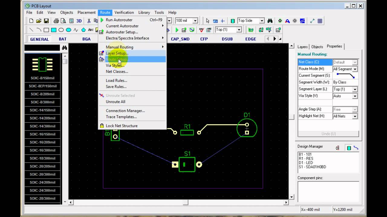
How to convert a schematic to a PCB Layout with PCB Creator - YouTube

Free PCB Schematic Entry & Layout Software Beat Eagle for Some Features

Analog To Digital Converter Circuit

From Idea to Schematic to PCB - How to do it easily! - YouTube

Teach you how to draw a simple PCB schematic in seven steps – So Good

How to Convert schematic diagram into PCB layout in Easyeda Online PCB

High Density PCB Layout of DC/DC Converters, Part 1 - Power management

High Density PCB Layout of DC/DC Converters, Part 2 - Power management
